Scanning Electron Microscopy | SEM Analysis Services
WHAT IS SEM ANALYSIS?
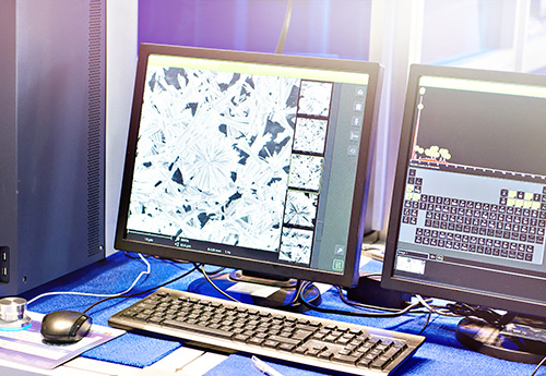
SEM Analysis (Scanning Electron Microscopy) consists of concentrating a focused beam of high-energy electrons, which generates a number of signals at the surface of solid specimens: metals, polymers, or composites. These signals, which are gleaned from electron-sample interactions, relay important information about the sample, such as texture, microstructure, the processes performed on the material during manufacture, and whether the material meets the needed specifications to ensure optimal durability in the intended application.
SEM Analysis is performed quickly and the microscopes used in this process are able to generate data in a sophisticated digital form.
SEM Analysis is used in research, quality control, and characterization for several industries including semiconductor manufacturing, biology, nanotechnology, forensics, geology, and materials science.
Benefits of SEM Analysis
Sample Versatility
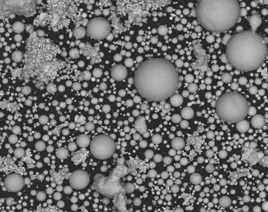
SEM can analyze a variety of materials, including powders, solid materials, coatings, biological specimens, and fibers.
3D and High-Resolution Imaging
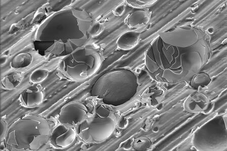
High-Resolution imaging provides a detailed visualization of surface features and a 3D representation of the sample surface is created by capturing many images at different angles.
Elemental Analysis
Elemental composition is revealed by using EDS (energy-dispersive X-ray spectroscopy) or WDS (wavelength-dispersive X-ray spectroscopy) detectors. EDS analysis is used to supplement the high resolution, high depth of field images with as elemental analysis of the materials in the image field.
For more information on IMR's SEM capabilities, or to request a quote, click on the buttons below.


METALLURGICAL LAB SERVICES
Carburization
Case Depth
Certified Weld Inspections
Coatings Evaluations
Coating Thickness by XRF, SEM, Cross Section
Case Depth
Depth of Decarburization
Determination of Delta Ferrite Content
Determination of Volume Fraction by Point Count
Effective Case Depth
Failure Analysis
Fastener Discontinuities
Fluorescent Impregnation of Porous Coatings
Fractography
Fracture Mechanics
Grain Size
Inclusion Content/Rating
Intergranular Attack
Intergranular Oxidation
Light Microscopy - Macro, Micro & SEM Photography
Macroetching
Microetching
Microhardness (Knoop, Vickers, MacroVickers)
Microstructure
Orientation in Microstructure
Particle Analysis (Distribution, ID, Size)
Phase Volume Determination
Pipeline Integrity
Plating Evaluations
Plating Thickness
Porosity of Metals, Ceramics & Composites
Prior Austenitic Grain Boundary Determination
Replication (ASTM E1351)
Quantitative Image Analysis
SEM Analysis
Surface Evaluation (Dubpernell Active Site Test ASTM B456 Appx 4)
Surface Topography
Thermal Spray Coating Analysis
Titanium Beta Transus Determination
Weld Qualification & Testing
SEM Imaging and Analysis
There have been many advances in SEM technology due to improvements in lens design, high-brightness electron sources, new detectors, and electronic signal processing. There are many different types of scanning electron microscopes designed for specific purposes ranging from routine morphological studies to high-speed compositional analyses.
SEM Imaging: Custom Solutions
If your needs for SEM analysis transcend conventional testing protocols, contact us to create a custom testing process.
RELEVANT ACCREDITATIONS
Click here for a complete list of accreditations and certifications for all IMR Test Labs locations.
FAQ's
Coatings, fibers, powders, solid materials and biological specimens can be tested with SEM Analysis.
Surface roughness, crystallographic information, topography, particle size, and elemental composition are all revealed through SEM analysis.
Analyses can be completed in as little as a few hours.


